onsemi QFET Type P-Channel P-Channel QFET MOSFET, 2.7 A, 500 V Enhancement, 3-Pin TO-220AB FQP3P50
- RS Stock No.:
- 671-5118
- Mfr. Part No.:
- FQP3P50
- Brand:
- onsemi

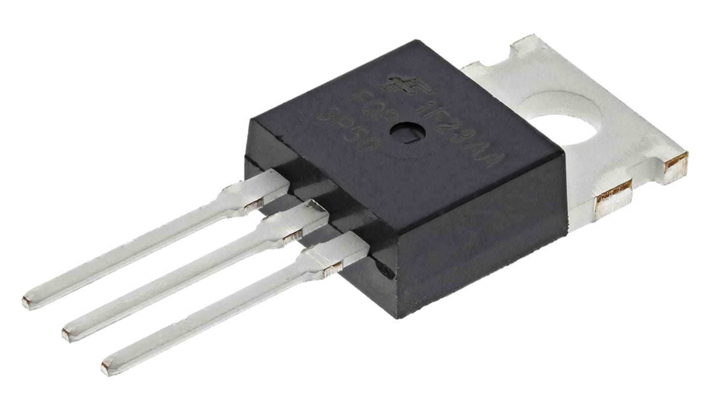
This image is representative of the product range
Stock information currently inaccessible
- RS Stock No.:
- 671-5118
- Mfr. Part No.:
- FQP3P50
- Brand:
- onsemi
Specifications
Technical data sheets
Legislation and Compliance
Product Details
Find similar products by selecting one or more attributes.
Select all | Attribute | Value |
|---|---|---|
| Brand | onsemi | |
| Series | QFET | |
| Channel Type | Type P | |
| Product Type | P-Channel QFET MOSFET | |
| Maximum Continuous Drain Current (Id) | 2.7 A | |
| Maximum Drain Source Voltage (Vds) | 500 V | |
| Channel Mode | Enhancement | |
| Pin Count | 3 | |
| Package Type | TO-220AB | |
| Automotive Standard | No | |
| Forward Voltage (Vf) | -5 V | |
| Height | 9.4 mm | |
| Length | 10.1 mm | |
| Maximum Drain Source Resistance (Rds) | 4.9 Ω | |
| Maximum Gate Source Voltage (Vgs) | 30 V | |
| Maximum Operating Temperature | 150 °C | |
| Maximum Power Dissipation (Pd) | 85 W | |
| Minimum Operating Temperature | 55 °C | |
| Mount Type | Through Hole | |
| Standards/Approvals | No | |
| Typical Gate Charge (Qg) @ Vgs | 18 nC | |
| Width | 4.7 mm | |
| Select all | ||
|---|---|---|
Brand onsemi | ||
Series QFET | ||
Channel Type Type P | ||
Product Type P-Channel QFET MOSFET | ||
Maximum Continuous Drain Current (Id) 2.7 A | ||
Maximum Drain Source Voltage (Vds) 500 V | ||
Channel Mode Enhancement | ||
Pin Count 3 | ||
Package Type TO-220AB | ||
Automotive Standard No | ||
Forward Voltage (Vf) -5 V | ||
Height 9.4 mm | ||
Length 10.1 mm | ||
Maximum Drain Source Resistance (Rds) 4.9 Ω | ||
Maximum Gate Source Voltage (Vgs) 30 V | ||
Maximum Operating Temperature 150 °C | ||
Maximum Power Dissipation (Pd) 85 W | ||
Minimum Operating Temperature 55 °C | ||
Mount Type Through Hole | ||
Standards/Approvals No | ||
Typical Gate Charge (Qg) @ Vgs 18 nC | ||
Width 4.7 mm | ||
QFET® P-Channel MOSFET, Fairchild Semiconductor
Fairchild Semiconductor’s new QFET® Planar MOSFETs use advanced, proprietary technology to offer best-in-class operating performance for a wide range of applications, including power supplies, PFC (Power Factor Correction), DC-DC Converters, Plasma Display Panels (PDP), lighting ballasts, and motion control.
They offer reduced on-state loss by lowering on-resistance (RDS(on)), and reduced switching loss by lowering gate charge (Qg) and output capacitance (Coss). By using Advanced QFET® process technology, Fairchild can offer an improved figure of merit (FOM) over competing Planar MOSFET devices.
MOSFET Transistors, ON Semi
ON Semi offers a substantial portfolio of MOSFET devices that includes high-voltage (>250V) and low-voltage (<250V) types. The Advanced silicon technology provides smaller die sizes, which it is incorporated into multiple industry-standard and thermally-enhanced packages.
ON Semi MOSFETs provide superior design reliability from reduced voltage spikes and overshoot, to lower junction capacitance and reverse recovery charge, to elimination of additional external components to keep systems up and running longer.
Related links
- onsemi QFET Type P-Channel P-Channel QFET MOSFET 500 V Enhancement, 3-Pin TO-220AB FQP3P50
- onsemi QFET Type P-Channel MOSFET 200 V Enhancement, 3-Pin TO-220
- onsemi QFET Type P-Channel MOSFET 200 V Enhancement, 3-Pin TO-220 FQPF7P20
- onsemi QFET Type P-Channel MOSFET 250 V Enhancement, 3-Pin TO-3PN
- onsemi QFET Type P-Channel MOSFET 100 V Enhancement, 3-Pin TO-252
- onsemi QFET Type P-Channel MOSFET 250 V Enhancement, 3-Pin TO-3PN FQA9P25
- onsemi QFET Type P-Channel MOSFET 100 V Enhancement, 3-Pin TO-252 FQD8P10TM
- onsemi QFET Type P-Channel MOSFET 500 V Enhancement, 3-Pin TO-252