Altera FPGA 5CEBA2 25000 Cells, 25000 Gates, 2002944 bit 9434 Blocks, 256-Pin FBGA
- RS Stock No.:
- 830-3540P
- Mfr. Part No.:
- 5CEBA2F17C8N
- Brand:
- Altera

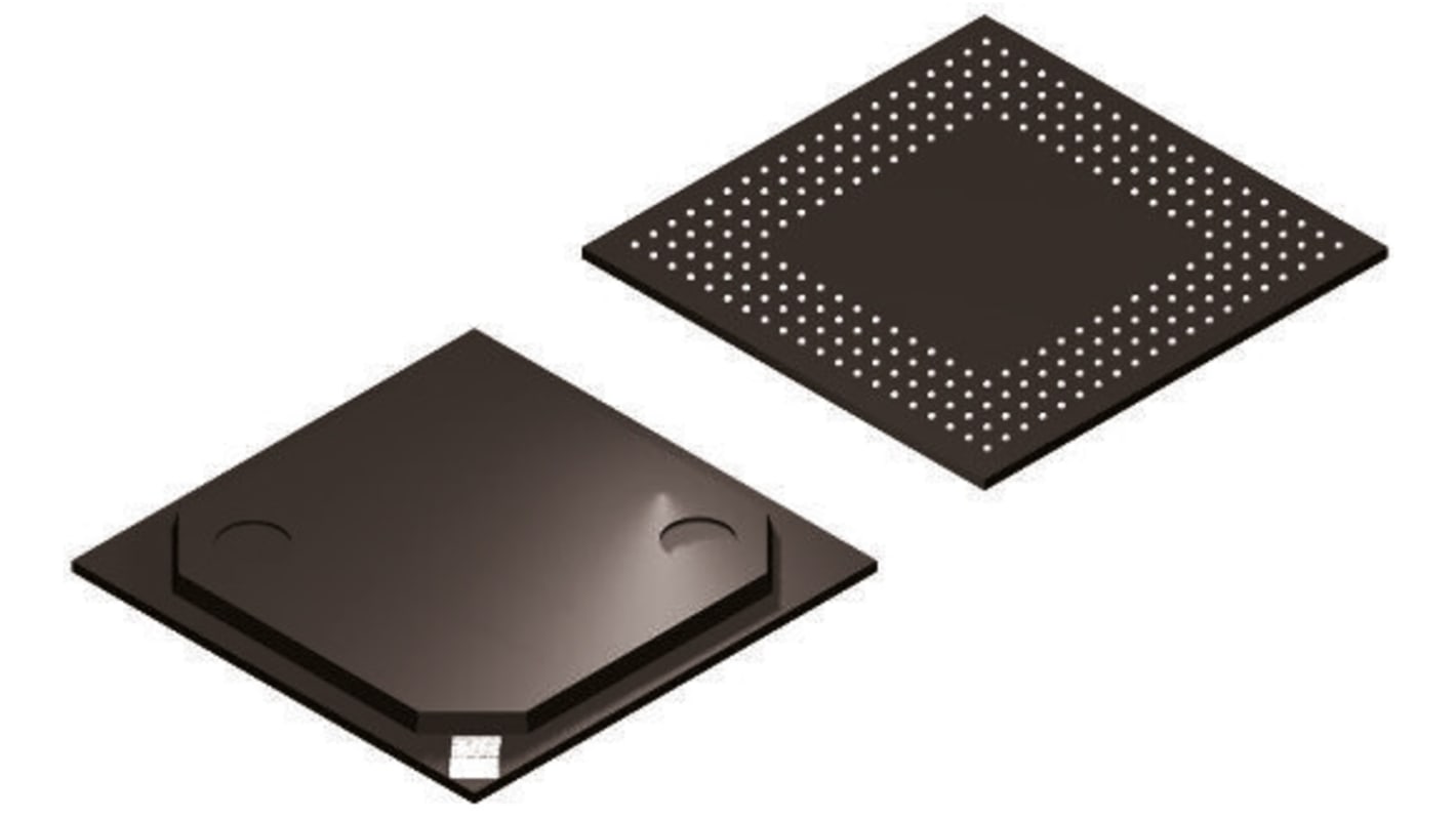
This image is representative of the product range
Currently unavailable
We don't know if this item will be back in stock, RS intend to remove it from our range soon.
- RS Stock No.:
- 830-3540P
- Mfr. Part No.:
- 5CEBA2F17C8N
- Brand:
- Altera
Specifications
Technical data sheets
Legislation and Compliance
Product Details
Find similar products by selecting one or more attributes.
Select all | Attribute | Value |
|---|---|---|
| Brand | Altera | |
| Series | 5CEBA2 | |
| Product Type | FPGA | |
| Number of Logic Gates | 25000 | |
| Number of Logic Cells | 25000 | |
| Number of Logic Units | 9434 | |
| Number of Registers | 37736 | |
| Number of Multipliers | 50 (18 x 18) | |
| Mount Type | Surface | |
| Package Type | FBGA | |
| Minimum Supply Voltage | 1.07V | |
| Pin Count | 256 | |
| Maximum Supply Voltage | 1.13V | |
| Minimum Operating Temperature | 0°C | |
| Number of RAM Bits | 2002944bit | |
| Number of I/Os | 128 | |
| Maximum Operating Temperature | 85°C | |
| Width | 17 mm | |
| Length | 17mm | |
| Standards/Approvals | No | |
| Automotive Standard | No | |
| Select all | ||
|---|---|---|
Brand Altera | ||
Series 5CEBA2 | ||
Product Type FPGA | ||
Number of Logic Gates 25000 | ||
Number of Logic Cells 25000 | ||
Number of Logic Units 9434 | ||
Number of Registers 37736 | ||
Number of Multipliers 50 (18 x 18) | ||
Mount Type Surface | ||
Package Type FBGA | ||
Minimum Supply Voltage 1.07V | ||
Pin Count 256 | ||
Maximum Supply Voltage 1.13V | ||
Minimum Operating Temperature 0°C | ||
Number of RAM Bits 2002944bit | ||
Number of I/Os 128 | ||
Maximum Operating Temperature 85°C | ||
Width 17 mm | ||
Length 17mm | ||
Standards/Approvals No | ||
Automotive Standard No | ||
Cyclone FPGA, Altera
An FPGA is a semiconductor device consisting of a matrix of Configurable Logic Blocks (CLBs) connected through programmable interconnects. The user determines these interconnections by programming SRAM. A CLB can be simple (AND, OR gates, etc) or complex (a block of RAM). The FPGA allows changes to be made to a design even after the device is soldered into a PCB.