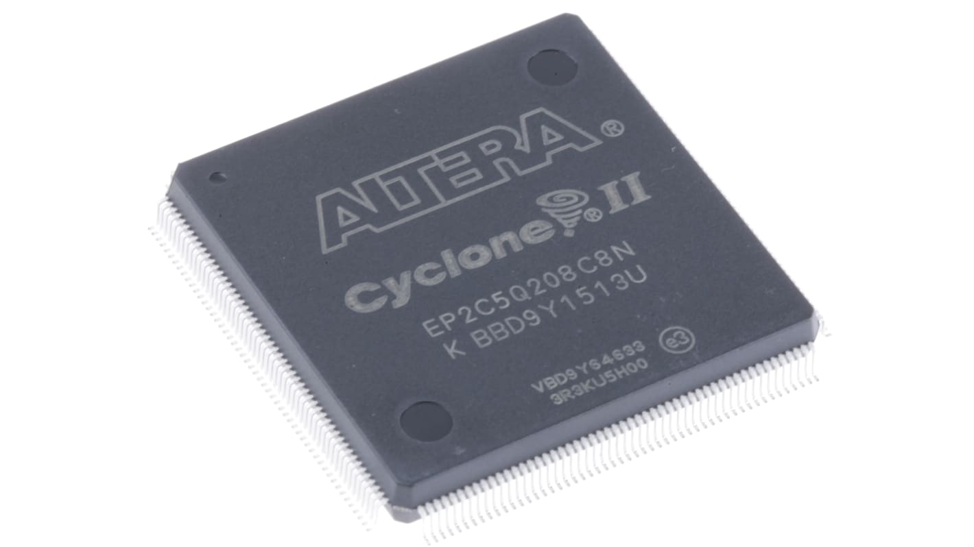
Altera FPGA Cyclone II 4608 Cells, 4608 Blocks, 208-Pin PQFP
- RS Stock No.:
- 624-4212
- Mfr. Part No.:
- EP2C5Q208C8N
- Brand:
- Altera

Currently unavailable
We don't know if this item will be back in stock, RS intend to remove it from our range soon.
- RS Stock No.:
- 624-4212
- Mfr. Part No.:
- EP2C5Q208C8N
- Brand:
- Altera
Specifications
Technical data sheets
Legislation and Compliance
Product Details
Find similar products by selecting one or more attributes.
Select all | Attribute | Value |
|---|---|---|
| Brand | Altera | |
| Series | Cyclone II | |
| Product Type | FPGA | |
| Number of Logic Cells | 4608 | |
| Number of Logic Units | 4608 | |
| Number of Multipliers | 13 | |
| Mount Type | Surface | |
| Package Type | PQFP | |
| Minimum Supply Voltage | 1.15V | |
| Pin Count | 208 | |
| Maximum Supply Voltage | 1.25V | |
| Minimum Operating Temperature | 0°C | |
| Maximum Operating Temperature | 85°C | |
| Standards/Approvals | No | |
| Height | 3.4mm | |
| Length | 28mm | |
| Automotive Standard | No | |
| Select all | ||
|---|---|---|
Brand Altera | ||
Series Cyclone II | ||
Product Type FPGA | ||
Number of Logic Cells 4608 | ||
Number of Logic Units 4608 | ||
Number of Multipliers 13 | ||
Mount Type Surface | ||
Package Type PQFP | ||
Minimum Supply Voltage 1.15V | ||
Pin Count 208 | ||
Maximum Supply Voltage 1.25V | ||
Minimum Operating Temperature 0°C | ||
Maximum Operating Temperature 85°C | ||
Standards/Approvals No | ||
Height 3.4mm | ||
Length 28mm | ||
Automotive Standard No | ||
Cyclone FPGA, Altera
An FPGA is a semiconductor device consisting of a matrix of Configurable Logic Blocks (CLBs) connected through programmable interconnects. The user determines these interconnections by programming SRAM. A CLB can be simple (AND, OR gates, etc) or complex (a block of RAM). The FPGA allows changes to be made to a design even after the device is soldered into a PCB.
Related links
- Altera FPGA Cyclone II 4608 Cells 144-Pin TQFP
- Altera FPGA EP2C8Q208C8N Cyclone II 8256 Cells 208-Pin PQFP
- Xilinx FPGA XC2S150-5PQG208C 150000 Gates 864 Blocks, 208-Pin PQFP
- Altera FPGA Cyclone IV 6272 Cells 144-Pin EQFP
- Altera FPGA Cyclone IV E 6272 Cells 276480 bit 392 Blocks, 256-Pin FBGA
- Altera FPGA Cyclone IV E 6272 Cells 276480 bit 392 Blocks, 144-Pin EQFP
- Altera FPGA Cyclone IV GX 14400 Cells 169-Pin FBGA
- FPGAs