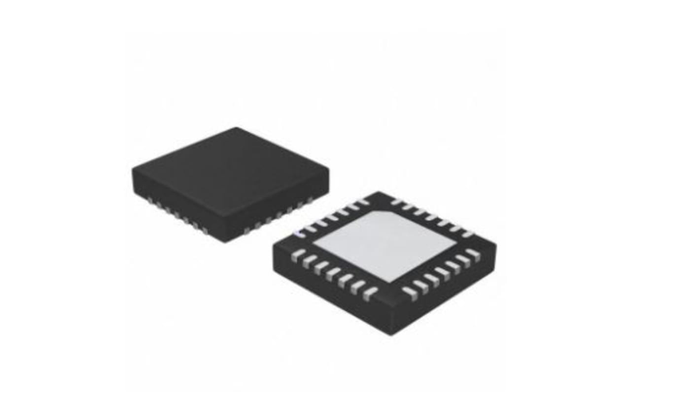
Renesas Electronics 5T9306NLGI Clock Buffer, 8-Pin 6 SOIC
- RS Stock No.:
- 216-6188
- Mfr. Part No.:
- 5T9306NLGI
- Brand:
- Renesas Electronics

This image is representative of the product range
Currently unavailable
We don't know if this item will be back in stock, RS intend to remove it from our range soon.
- RS Stock No.:
- 216-6188
- Mfr. Part No.:
- 5T9306NLGI
- Brand:
- Renesas Electronics
Specifications
Technical data sheets
Legislation and Compliance
Product Details
Find similar products by selecting one or more attributes.
Select all | Attribute | Value |
|---|---|---|
| Brand | Renesas Electronics | |
| Product Type | Clock Buffer | |
| Mount Type | Surface | |
| Package Type | SOIC | |
| Minimum Supply Voltage | 2.3V | |
| Pin Count | 8 | |
| Maximum Supply Voltage | 2.7V | |
| Minimum Operating Temperature | -40°C | |
| Maximum Operating Temperature | 85°C | |
| Series | 5T9306 | |
| Length | 6mm | |
| Standards/Approvals | No | |
| Height | 0.8mm | |
| Width | 6 mm | |
| Maximum Output Frequency | 1GHz | |
| Automotive Standard | No | |
| Number of Outputs | 6 | |
| Select all | ||
|---|---|---|
Brand Renesas Electronics | ||
Product Type Clock Buffer | ||
Mount Type Surface | ||
Package Type SOIC | ||
Minimum Supply Voltage 2.3V | ||
Pin Count 8 | ||
Maximum Supply Voltage 2.7V | ||
Minimum Operating Temperature -40°C | ||
Maximum Operating Temperature 85°C | ||
Series 5T9306 | ||
Length 6mm | ||
Standards/Approvals No | ||
Height 0.8mm | ||
Width 6 mm | ||
Maximum Output Frequency 1GHz | ||
Automotive Standard No | ||
Number of Outputs 6 | ||
The Renesas Electronics IDT5T9306 2.5V differential clock buffer is a user-selectable differential input to six LVDS outputs. The fanout from a differential input to six LVDS outputs reduces loading on the preceding driver and provides an efficient clock distribution network. The IDT5T9306 can act as a translator from a differential HSTL, eHSTL, LVEPECL (2.5V), LVPECL (3.3V), CML, or LVDS input to LVDS outputs. A single-ended 3.3V / 2.5V LVTTL input can also be used to translate to LVDS outputs.
Guaranteed Low Skew < 40ps (max)
Very low duty cycle distortion < 125ps (max)
High speed propagation delay < 1.75ns (max)
Additive phase jitter, RMS 0.159ps (typical) @ 125MHz
Up to 1GHz operation
Selectable inputs
Hot insertable and over-voltage tolerant inputs
3.3V / 2.5V LVTTL, HSTL, eHSTL, LVEPECL (2.5V), LVPECL
(3.3V), CML, or LVDS input interface
Selectable differential inputs to six LVDS outputs
Power-down mode
2.5V VDD
Available in VFQFPN package
Related links
- Renesas Electronics 5T9306NLGI Clock Buffer, 8-Pin 6 SOIC
- Renesas Electronics 854S006AGILF Clock Buffer, 24-Pin 6 SOIC
- Renesas Electronics 553SCMGI Clock Buffer, 8-Pin 4 SOIC
- Renesas Electronics 551MILF Clock Buffer, 8-Pin 4 SOIC
- Renesas Electronics 524MILF Clock Buffer, 8-Pin 4 SOIC
- Renesas Electronics 553MILF Clock Buffer, 8-Pin 4 SOIC
- Renesas Electronics 553MILFT Clock Buffer, 8-Pin 4 SOIC
- Renesas Electronics 83026BGI-01LF Clock Buffer, 8-Pin 2 SOIC
