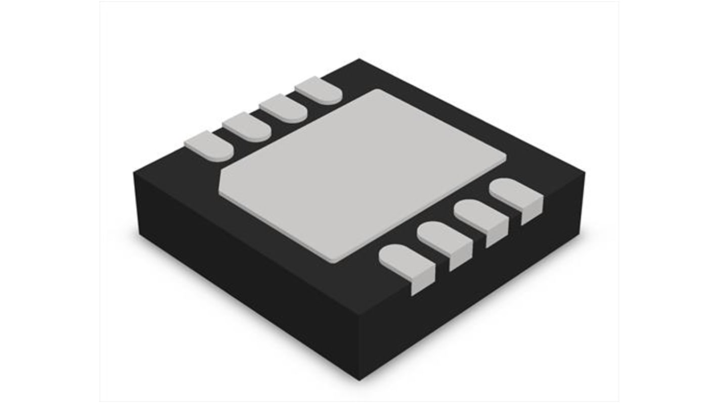
Renesas Electronics 5PB1104CMGK Clock Buffer, 8-Pin 4 DFN
- RS Stock No.:
- 216-6171
- Mfr. Part No.:
- 5PB1104CMGK
- Brand:
- Renesas Electronics

This image is representative of the product range
Currently unavailable
We don't know if this item will be back in stock, RS intend to remove it from our range soon.
- RS Stock No.:
- 216-6171
- Mfr. Part No.:
- 5PB1104CMGK
- Brand:
- Renesas Electronics
Specifications
Technical data sheets
Legislation and Compliance
Product Details
Find similar products by selecting one or more attributes.
Select all | Attribute | Value |
|---|---|---|
| Brand | Renesas Electronics | |
| Product Type | Clock Buffer | |
| Mount Type | Surface | |
| Package Type | DFN | |
| Minimum Supply Voltage | 1.8V | |
| Pin Count | 8 | |
| Maximum Supply Voltage | 3.3V | |
| Minimum Operating Temperature | -40°C | |
| Maximum Operating Temperature | 105°C | |
| Height | 0.5mm | |
| Length | 2mm | |
| Width | 2 mm | |
| Standards/Approvals | No | |
| Series | 5PB1104 | |
| Maximum Output Frequency | 200MHz | |
| Automotive Standard | AEC-Q100 | |
| Number of Outputs | 4 | |
| Select all | ||
|---|---|---|
Brand Renesas Electronics | ||
Product Type Clock Buffer | ||
Mount Type Surface | ||
Package Type DFN | ||
Minimum Supply Voltage 1.8V | ||
Pin Count 8 | ||
Maximum Supply Voltage 3.3V | ||
Minimum Operating Temperature -40°C | ||
Maximum Operating Temperature 105°C | ||
Height 0.5mm | ||
Length 2mm | ||
Width 2 mm | ||
Standards/Approvals No | ||
Series 5PB1104 | ||
Maximum Output Frequency 200MHz | ||
Automotive Standard AEC-Q100 | ||
Number of Outputs 4 | ||
The Renesas Electronics 5PB11xx is a high-performance LVCMOS clock buffer family of devices. It has an additive phase jitter of 50fs RMS. There are five different fan-out variations available: 1:2 to 1:10. The 5PB11xx supports a synchronous glitch-free output enable (OE) function to eliminate any potential intermediate incorrect output clock cycles when enabling or disabling outputs. It can operate from a 1.8V to 3.3V supply.
High-performance 1:2, 1:4, 1:6, 1:8, 1:10 LVCMOS clock buffer
Very low pin-to-pin skew: < 50ps
Very low additive jitter: < 50fs
Supply voltage: 1.8V to 3.3V
3.3V tolerant input clock
fMAX = 200MHz
Integrated serial termination for 50Ω channel
Related links
- Renesas Electronics 5PB1104CMGK Clock Buffer, 8-Pin 4 DFN
- Renesas Electronics 5PB1104CMGI Clock Buffer, 8-Pin 4 DFN
- Renesas Electronics 553SCMGI Clock Buffer, 8-Pin 4 SOIC
- Renesas Electronics 551MILF Clock Buffer, 8-Pin 4 SOIC
- Renesas Electronics 524MILF Clock Buffer, 8-Pin 4 SOIC
- Renesas Electronics 553MILF Clock Buffer, 8-Pin 4 SOIC
- Renesas Electronics 553MILFT Clock Buffer, 8-Pin 4 SOIC
- Renesas Electronics 74FCT38074SDCGI Clock Buffer, 8-Pin 4 SOIC
