Lattice Semiconductor iCE40LP1K-BLINK-EVN iCEblink40 Evaluation Kit iCEblink40-LP1K

- RS Stock No.:
- 771-9433
- Mfr. Part No.:
- iCE40LP1K-BLINK-EVN
- Brand:
- Lattice Semiconductor
Available for back order.
Added
Price (ex. GST) Each
$348.67
(exc. GST)
$383.54
(inc. GST)
| Units | Per unit |
| 1 + | $348.67 |
- RS Stock No.:
- 771-9433
- Mfr. Part No.:
- iCE40LP1K-BLINK-EVN
- Brand:
- Lattice Semiconductor
Technical data sheets
Legislation and Compliance
Product Details
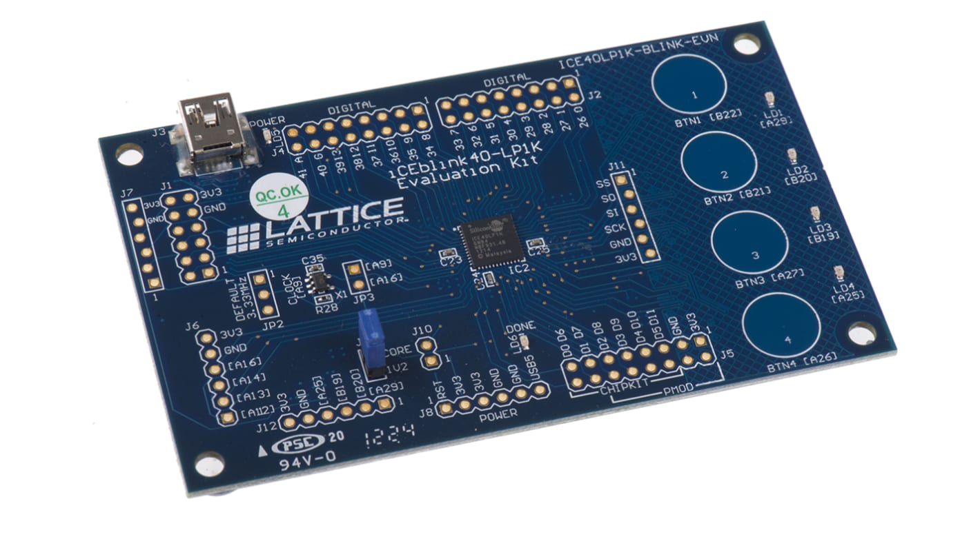
Lattice iCEblink40-LP1K Evaluation Kit
A low-cost platform for evaluating and developing with the low-power iCE40LP1K FPGA. The board provides access to general-purpose I/O and includes capacitive-touch buttons and LEDs. The board is powered and programmed via USB. An on-board microcontroller enables 2-way communication with the iCE40LP1K FPGA. The free iCEcube2™ development tool controls programming, accesses virtual I/O functions and runs the included demos. The tools can be downloaded from the Lattice website.
Low-power, small-footprint iCE40LP1K FPGA in 84-pin QFNS package
USB programming, debugging, virtual I/O functions, and power supply
4 x User LEDs
4 x Capacitive-touch buttons
3.3MHz clock source
1Mbit SPI serial configuration PROM
Supported by Lattice iCEcube2 design software
63 x LVCMOS/LVTTL (3.3V) digital I/O connections on 0.1in through-hole connections
Supports third-party I/O expansion boards and modules, including 3.3V Arduino Shield boards (requires additional sockets, not supplied)
Supplied with
USB cable for power & programming, QuickStart Guide
An FPGA is a semiconductor device consisting of a matrix of Configurable Logic Blocks (CLBs) connected through programmable interconnects. The user determines these interconnections by programming SRAM. A CLB can be simple (AND, OR gates, etc) or complex (a block of RAM). The FPGA allows changes to be made to a design even after the device is soldered into a PCB.
Specifications
Attribute | Value |
|---|---|
| Programmable Logic Technology | FPGA |
| Kit Classification | Evaluation Kit |
| Featured Device | iCEblink40-LP1K |
| Kit Name | iCEblink40 |
Related links
- Lattice Semiconductor LC4032V-75TN44C 30 I/O 7.5ns 44-Pin TQFP
- Lattice Semiconductor LCMXO2-4000HC-4TG144I 4320 Labs ISP, 144-Pin TQFP
- Lattice Semiconductor LCMXO2-7000HC-4TG144I 6864 Labs ISP, 144-Pin TQFP
- Texas Instruments Motor Driver Evaluation Kit
- Skyworks Solutions Inc Si85853-KIT Si85853D Evaluation Kit...
- Microchip AT42QT1010 Evaluation Kit Evaluation Kit for AC160219
- Bosch Sensortec BME688 EVALUATION KIT BOARD Evaluation Board...
- Sensirion SEK-SFM3xxx-AW/D Evaluation Kit Cable Evaluation Kit for...